Detector Development
To explore the physics of proton or lead ion collisions at the LHC and to test theories such as Quantum Chromodynamics (QCD) or examine the evolution and properties of the so-called Quark-Gluon Plasma (see Data Analysis and Phenomenology sections), we employ particle detectors, devices able to reconstruct the passage of particles. Their purpose is to track and identify charged particles produced and emerging from the collision point. Often, multiple detector types are combined to create larger systems, such as the ALICE experiment, in order to enhance performance. Several factors define the performance of the detector: the resolution and efficiency of measurements, the ability to handle high rates of particle interactions, the ability to withstand and function accurately in high-radiation environments, quick response times and low levels of noise.
Ideally, a detector would offer unlimited precision for the variables of interest. However, in reality, the particles need to interact with the detector material to generate a readable signal. Therefore, the detector itself impacts the measurement, imposing inherent limits on the measurement precision. To achieve the highest levels of precision and continuously improve the design, Research and Development (R&D) of new detectors and technologies never stops. Whether existing detectors are being upgraded or new ones are being built, there is always work to be done.
At the heart of the experiment, near the interaction vertex, a silicon detector is the only viable technology that provides the required spatial resolution and speed to effectively resolve the high amount of particles produced during collisions. This detector must also maintain reliable operation over extended periods despite substantial radiation exposure and other demanding conditions. Pixel sensors are particularly well-suited for these demands and are as such employed in the upgraded Inner Tracking System (ITS) of ALICE.
Our group focuses on silicon pixel detectors, particularly Monolithic Active Pixel Sensors (MAPS), fabricated using CMOS technology. MAPS integrate signal-processing electronic circuits within each pixel, enabling tasks such as signal amplification and discrimination to be performed directly inside each pixel. We employ two generations of MAPS, each accompanied by a range of ancillary components.
Methodology
Once a new detector is designed and fabricated, it must undergo testing to verify its functionality and performance, ensuring it operates as intended and to evaluate its performance under different modes of operation. This involves a battery of tests, some conducted in our laboratory and others at particle accelerator facilities during so-called beam tests campaigns.
To enhance our understanding of these detectors, we conduct dedicated simulations, based on our current operational principles of the detector. By comparing these simulations with actual experimental data, we can assess the accuracy of our models and refine our current understanding of the detectors.
Laboratory Measurements
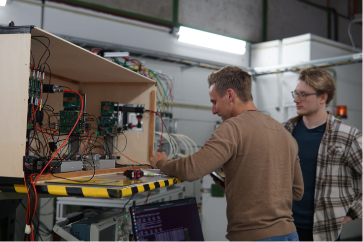
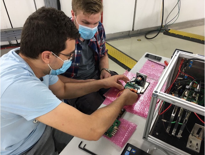
Our laboratory is equipped to test new sensors immediately after bonding. We investigate the readout electronics, perform power tests and analyze the electrical circuits to determine their functionality and behavior, going from particle detection to the sensor readout. Furthermore, we determine the optimal working point of the sensors through precise tuning of the operational parameters, we study the effects of radiation-induced damage on the performance of the sensors and we calibrate their response using radioactive sources, among other activities. Finally, we integrate the single sensors in complex setups for dedicated measurements.
Besides testing sensors, our daily laboratory work also involves developing and maintaining the infrastructure for these measurements.
This includes the
Beam Tests
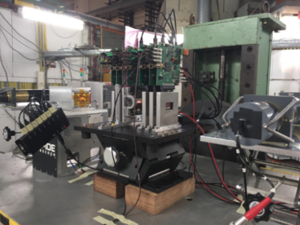
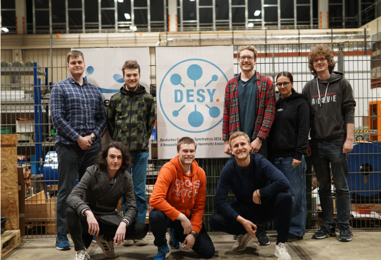
To investigate the performance of the sensor in greater detail, we study parameters of interest (e.g. the detection efficiency, position resolution, etc. ) at dedicated beam test facilities. During such campaigns the sensors under test are exposed to a particle beam at an accelerator facility like GSI, CERN, DESY, MIT and CCB (Krakow). The sensors are integrated into a beam telescope (sequential array of pixel sensors with known behavior), allowing a precise benchmarking. By comparing their response with reference detectors, the quantities of interest can be extracted from the data taken through detailed analysis.
Our group is engaged in the complete process of sensor characterization, beginning with preparatory lab work, followed by data acquisition conducted at a beam test and concluding with the comprehensive data analysis phase afterwards.
Simulation
We use the Allpix2 framework to simulate the response of detectors, encompassing the entire process from the impact of the incident ionizing radiation to the digitization of hits in the detector. These simulations allow us to test our knowledge of the in-pixel dynamics and by comparing them to the actual measurements taken with the real detector, we can better understand the myriad of effects at play.
In addition, Geant4 simulations are utilized to understand effects observed in the entire measurement setup (i.e. properties of the particle beam or geometric effects related to the mechanical setup). These simulations model the passage of particles through materials, providing valuable insights into data obtained at beam tests.
We also use simulations to investigate the physics processes relevant for future measurements or understand corrections needed for the testbeam data. By testing different hypotheses for the observed effects, we can comprehend the consequences of various decisions on test setups and optimize these setups for accurate measurements in the future.
Past Projects and Current Research
ALICE TPC Upgrade and GEM Studies
In the past, our group played a major role in the upgrade of the ALICE Time Projection Chamber (TPC). The readout chambers were changed from Multi-Wire Proportional Chambers (MWPC) to Gas Electron Multiplier (GEM)
based chambers. The group was mainly involved in the effort of
ALPIDE Testing
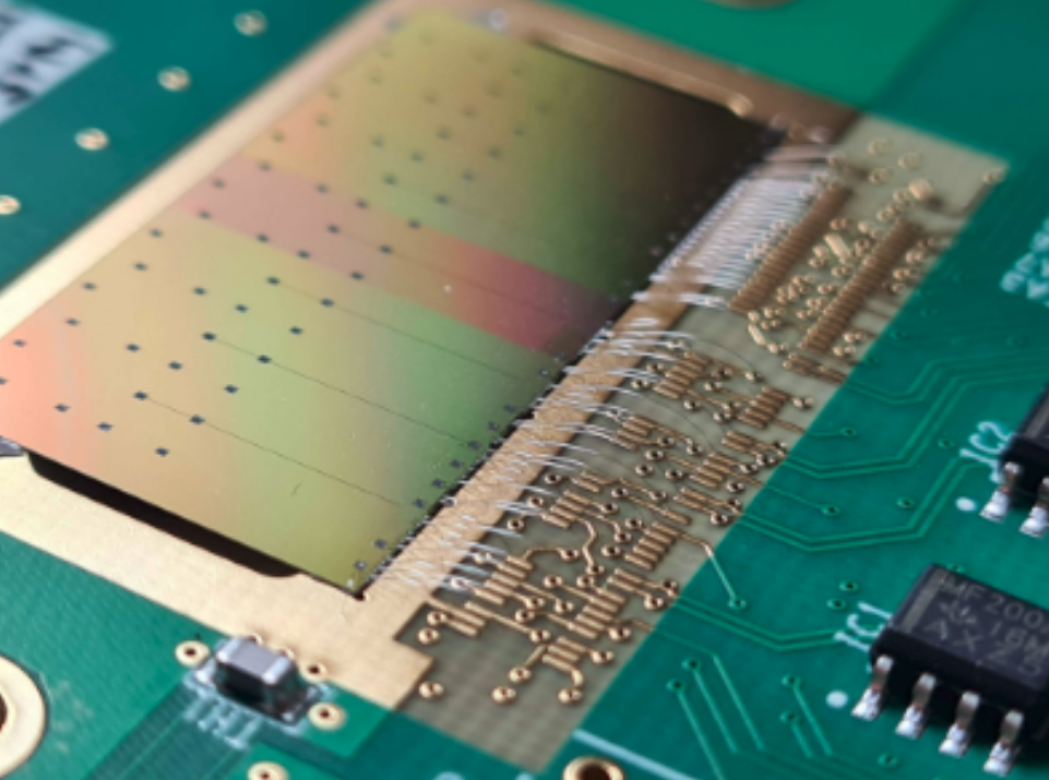
The Alice Pixel DEtector (ALPIDE) is a MAPS which has been developed for the upgrade of the ALICE Inner Tracking System (ITS). It features 1024 ⨯ 512 pixels for a total surface of about 3 ⨯ 1.5 cm2,. It boasts an excellent efficiency (>99.9%) at low noise levels (≪ 10-6 /px/event) and an intrinsic position resolution of better than 5 μm. The ALPIDE is currently successfully operating in the largest pixel detector with a sensitive area of 10m2, 24120 individual sensors and in total about 12.5 Gpixels.
After the fabrication of a chip, it needs to be interfaced with the outside world. This involves electrically connecting the on-chip input and output pads to a printed circuit board (PCB) to enable communication
with the sensor, a process known as bonding. Our group is involved in the
ALPIDE Applications
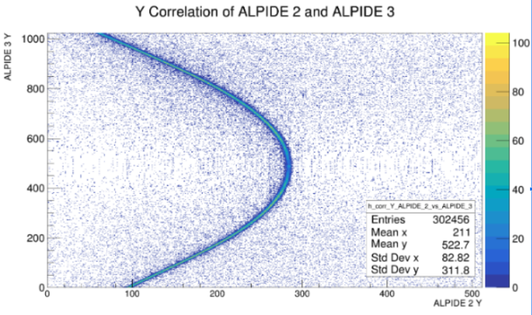
Several dedicated measurements using ALPIDE sensors have been performed in our group. The measurement of the rate and angular dependence of cosmic muons [7], alongside alignment and tracking 8][ of the muons has been performed in a series of measurements. Additionally, simulations using a simple theoretical model of charge drift and diffusion in the ALPIDE sensor have been performed to explore the potential of clustering as a proxy for rudimentary stand-alone particle identification [9].
Tracking low momentum heavy particles presents challenges due to the predominance of multiple scattering, which renders simple straight-line trajectories ineffective. To address this, dedicated studies on tracking low momentum protons using datasets taken at the CCB accelerator in Krakow were performed, comparing different track models [10]. Moreover, in-depth studies for the measurement of the reaction cross-section of low momentum protons were performed pending a dedicated testbeam campaign [11]. They offered an insight into the physics corrections needed for the data taken with ALPIDE sensors, as well as considerations for the setup configuration. A validation with a set of low statistics data was already performed.
Finally, large area modules (comprising 2⨯7 ALPIDE sensors), similar to the ones used in the ITS2, are also investigated in our group. They allow us to extend the acceptance of our setups and serve as an improved cosmics telescope, given their extended area. We are developing a full readout and DAQ chain for these sensors and validate their response with testbeam data [12].
Curved Silicon Sensors
Construction of a beam telescope
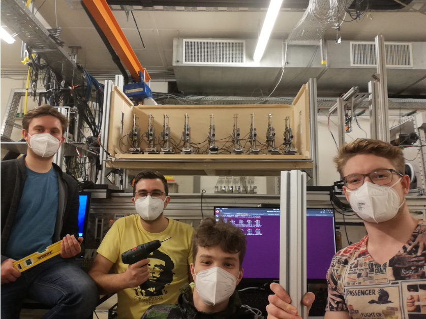
Our group has designed and built an affordable, modular, and highly flexible beam telescope capable of accommodating a large number of sensors and ancillary components. The entire setup is based on a rail system, allowing for quick and easy adjustments along all three major axes of translation for each individual sensor plane, groups of planes (upstream/downstream reference arms), or the entire telescope. The default precision is approximately 1mm in each direction, which can be significantly improved with the use of micrometer screws.
The design also allows for rotations around the vertical axis for each plane, enabling the study of the impact of inclined beam tracks relative to the sensor. Additionally, the new design easily integrates various other detectors or targets at any point along the beam direction. With this system, transporting the equipment becomes straightforward, setup times are drastically reduced due to its modular nature, and sensor alignment can be accomplished in a matter of minutes. This telescope has already been tested on numerous test beams, where the team has gained experience in fully operating the telescope alongside the DAQ hardware and software. Leveraging the experience of this setup, other more compact variants for use as a compact cosmics detector were also built and are operational in the laboratory.
65 nm CMOS Technology
To meet the requirements for the ITS3 upgrade of ALICE, the Material Budget Studies
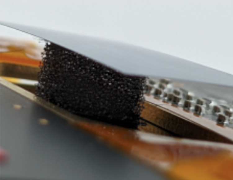
The open-cell carbon foam support structures in the ITS3 upgrade of ALICE are designed to support the cylindrical wafer-scale sensors, ensuring they remain in place with a consistent bending radius. The amount of material used is crucial: while more material offers better support, it also increases scattering, which negatively impacts the detector performance, especially at low momenta. To ensure high-efficiency track reconstruction, understanding the minimal scattering introduced by these supports is essential. Our group conducted dedicated measurements using material budget imaging techniques pioneered at DESY to assess the scattering effects of carbon foam wedges on spatial resolution [14] [18].
Stitched sensors: MOSS and babyMOSS
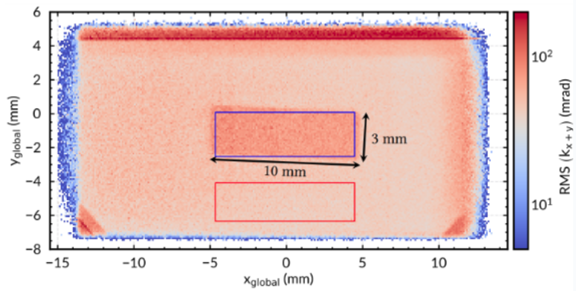
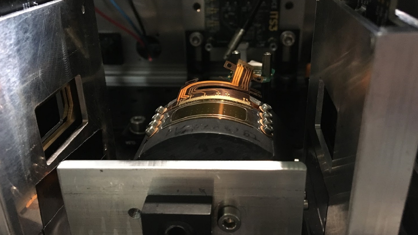
Following the successful qualification of the 65 nm technology, the next step towards the ITS3 upgrade of ALICE is to evaluate large area sensors produced with a technique known as stitching. This method enables integration of multiple individual single-sensor units directly on the silicon, forming larger pixel sensors that approach the size of a full silicon wafer. The first prototype of a stitched sensor, named Monolithic Stitched Sensor (MOSS), is currently undergoing testing to assess its feasibility, performance and yield [19].
Alongside the full stitched sensor, that encompasses 10 single-sensor repeated units, the large design exercise included smaller stitched units, known as babyMOSS. These sensors are of a similar size to an ALPIDE sensor and are also investigated by our team, in collaboration with CERN and Bonn groups [17] [18]. Current tests include an array of laboratory qualification tests, as well as analysis of beam test data.
Tools for Data Acquisition and Analysis
A significant amount of software is involved in detector research, primarily
Contact Persons in the Group
Bogdan Blidaru (PhD student)
Pascal Becht (PhD student)
Marius Menzel (PhD student)
Bent Buttwil (Master student)
Maurice Donner (Master student)
Simon Groß-Bölting (Master student)
Anouk Kaiser (Master student)
Johannes Hensler (Master student, HiWi)
Fabian Königstein (Master student, HiWi)
Sarah Michel (Bachelor student)


